Challenge
S parameter data are very useful to estimate the insertion loss and return loss. Many applications require S-parameter measurements between ASIC pads and SMA connector.
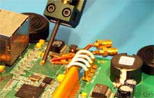
Engineers may consider using differential probe without any ground pin to capture mixed- mode S parameters and differential-mode impedance.
S Parameter Measurement Tips
- Use the the calibration substrate and probe provided by the same vendor to avoid calibration error
- Always check the calibration using short transmission line on calibration substrate
- Probing structure designs should be included in the PCB or package final release check list. Too many designers ignore this requirement and can't extract S parameter in lab due to missing adjacent ground pin or missing deemed structures.
- A missing ground pad at the ASIC area can prevent S-parameter measurement.
- Add simple through structure as a validation coupon to verify the loss effect of the stack up material.
- The phase value of a pair of differential traces provides useful information to detect the resonance beyond 7 GHz due to bad FR4 material.
Helpful links
Differential SS probe for SDD21 measurement
Differential probing without ground pin is easier than traditional GSSG probing. Since SS differential probe only has only two probe tips, positive and negative, one can easily make a good contact for vertical probing, double-side probing, PCB or package probing without ground pads.
Because the return currents of the two opposite probes flow through the probe coaxial external shell, they are cancelled at the probe tips with a good ground connection close to the tips. SS probe can measure TDR differential impedance or differential SDD21 and SDD11 with a VNA.
S Parameter Probing Demonstrations

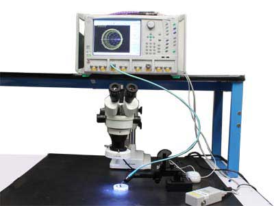
S-parameter calibration with substrate and VNA

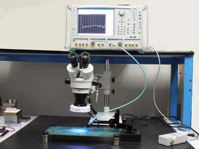
Parameter measurement on high-speed trace with VNA


