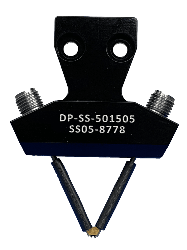
S-PROBE
High-Performance Rugged Probes for RF & SI Probing
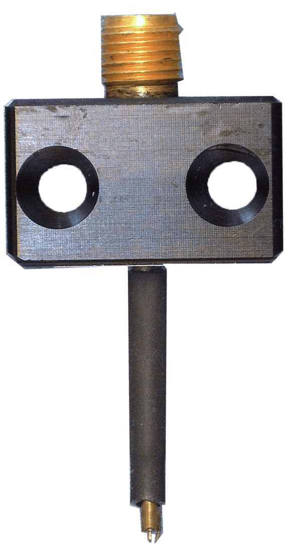
S-Probe series is designed for RF, signal integrity, and power integrity testing of printed-circuit boards. Microprobes are not suitable for this type of measurements due to their fragility.
HIGHLIGHTS
- High Bandwidth: DC to 30 GHz
- Low Insertion Loss: < 3 dB @ 30 GHz for probe pitch < 0.5 mm
- Ruggedness: Strong enough for direct probing test pads on uneven surfaces
- High Repeatability: No moving parts
- Probe-tip Calibration: Acurate measurements without the need of a soldering semi-rigid RF cables
- User experience similar to that of a microprobe
| Specifications | |
|---|---|
| Bandwidth | 30/20 GHz (0.25/0.4/0.5 mm pitch) 18 GHz (0.8/1.0 mm pitch) 16 GHz (1.2/1.4/1.6 mm pitch) |
| Insertion Loss | < 3 dB @ Bandwidth |
| Impedance | 50±2 Ohm |
| Connector Type | Female 2.92 mm/30 GHz, Female SMA/20 GHz |
| Dimensions (LxWxH) | 38 x 20 x 12 mm (1.5x0.8x0.5 in.) |
| Weight | 8 gm |
20 GHz S-Probe
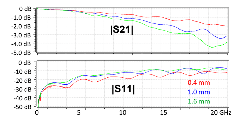
Un-calibrated S21/S11 for 0.4/1.0/1.6 mm pitch
| PART NO. | BW (GHz) | PROBE PITCH |
|---|---|---|
| SP-GR-2015025 | 20 GHz | 0.25 mm / 10 mil |
| SP-GR-201504 | 20 GHz | 0.4 mm / 16 mil |
| SP-GR-201505 | 20 GHz | 0.5 mm / 20 mil |
| SP-GR-181508 | 18 GHz | 0.8 mm / 32 mil |
| SP-GR-181510 | 18 GHz | 1.0 mm / 40 mil |
| SP-GR-161512 | 16 GHz | 1.2 mm / 48 mil |
| SP-GR-161514 | 16 GHz | 1.4 mm / 56 mil |
| SP-GR-161516 | 16 GHz | 1.6 mm / 64 mil |
30 GHz S-Probe
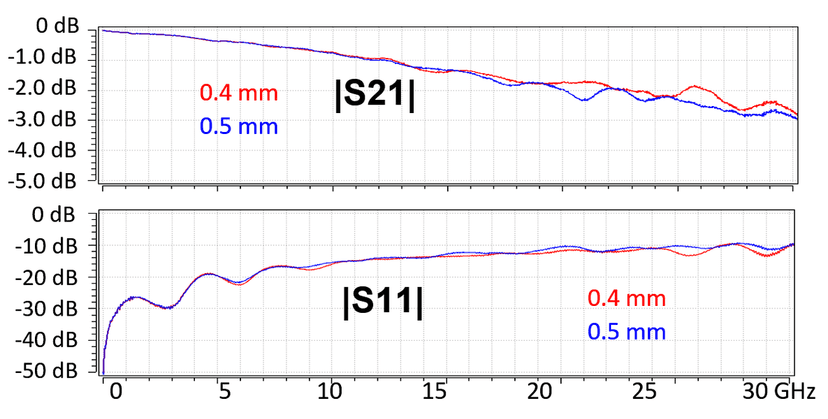
Un-calibrated S21/S11 for 0.4/0.5 mm pitch
| PART NO. | BW (GHz) | PROBE PITCH |
|---|---|---|
| SP-GR-3015025 | 30 GHz | 0.25 mm / 10 mil |
| SP-GR-301504 | 30 GHz | 0.4 mm / 16 mil |
| SP-GR-301505 | 30 GHz | 0.5 mm / 20 mil |
| PROBE PITCH VS. COMPONENT SIZE | |
|---|---|
| PROBE PART NO. | SIZE |
| SP-GR-2015025 | 01005 |
| SP-GR-201505 | 0201 |
| SP-GR-181510 | 0402 |
| SP-GR-161514 | 0603 |
Accessories
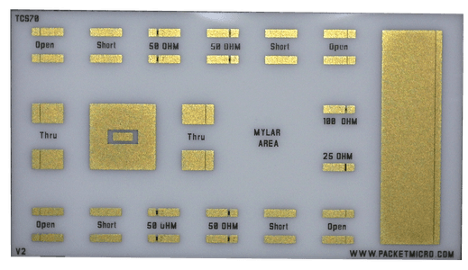
TCS70
CALIBRATION SUBSTRATE
S-Probe product family includes a TCS50 calibration substrate with short, open, load, and thru (SOLT) standards for S-parameter calibrations. This substrate enables a user to move the measurement reference point directly to the probe tips for accurate, repetitive testing.
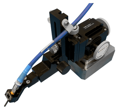
TP250 Precision Positioner
A precision positioner works with all PacketMicro's DIY probing fixtures.
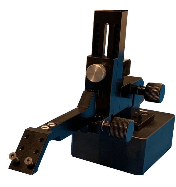
TP150 Precision Positioner
A low-cost positioner is good for simple, standalone probing measurements.
Applications
2 Sided Probing
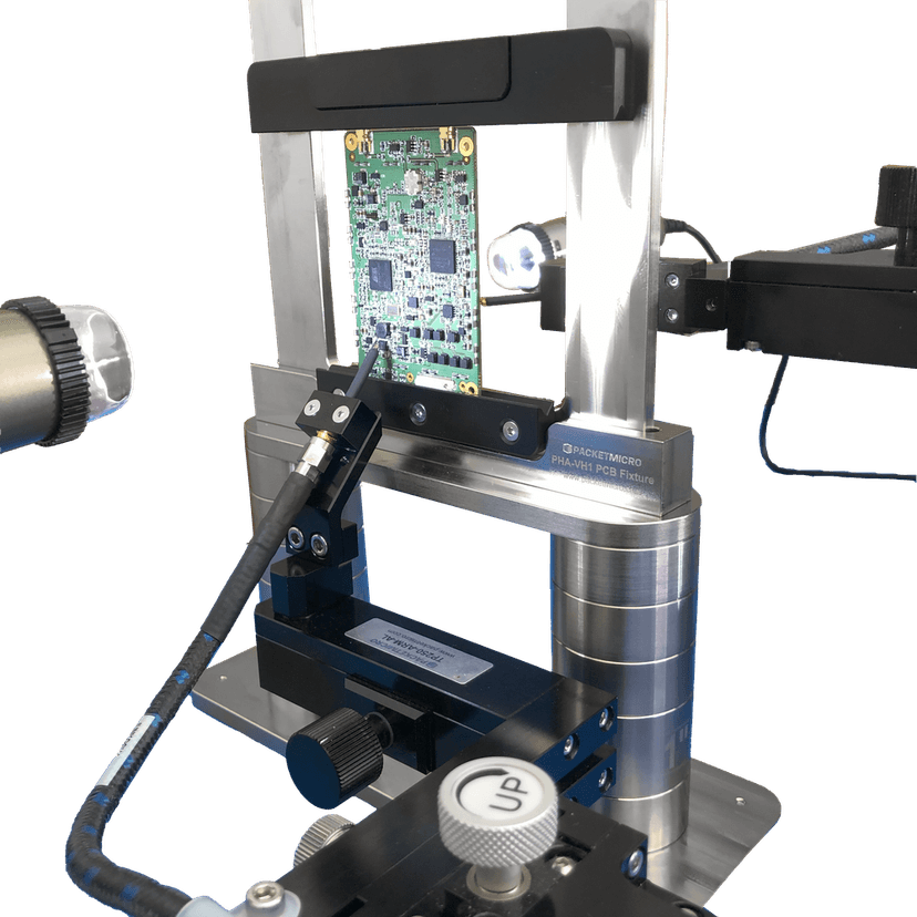
RF Socket Probing
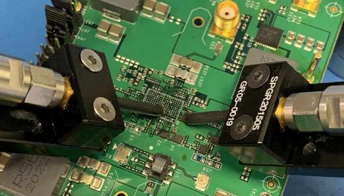
Check out our other Probes
R-PROBE
D-PROBE
