HPS24RP HORIZONTAL
PROBE STATION
DIY PCB PROBE STATTION FOR 1-SIDED & 2-SIDED PROBING
Easy to setup
and configure
Compact and
lightweight
Fast lock and unlock
magnetic switches
HIGHLIGHTS
- Rolling platform with sliders for holding PCBs up to 24"
- Horizontal rails for 1 & 2-sided probing with unconstrained PCB width
- Adjustable holders with magnetic base for secure PCB mounting
- Flexible manipulators with XYZ stage and planarization knob
- Easy, quick arrangement of positioners with a switchable magnetic base
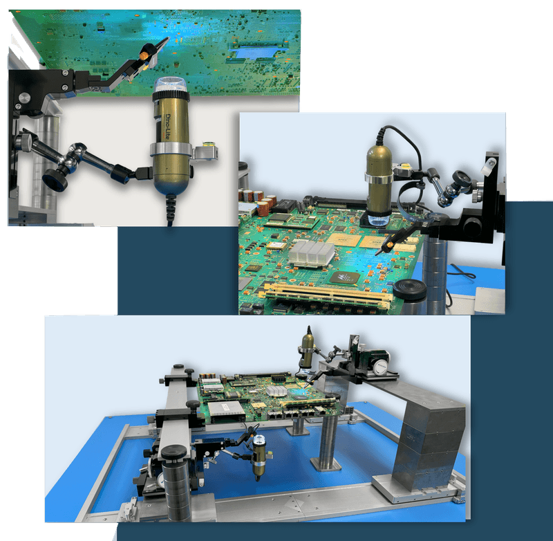
HPS24RP FEATURES
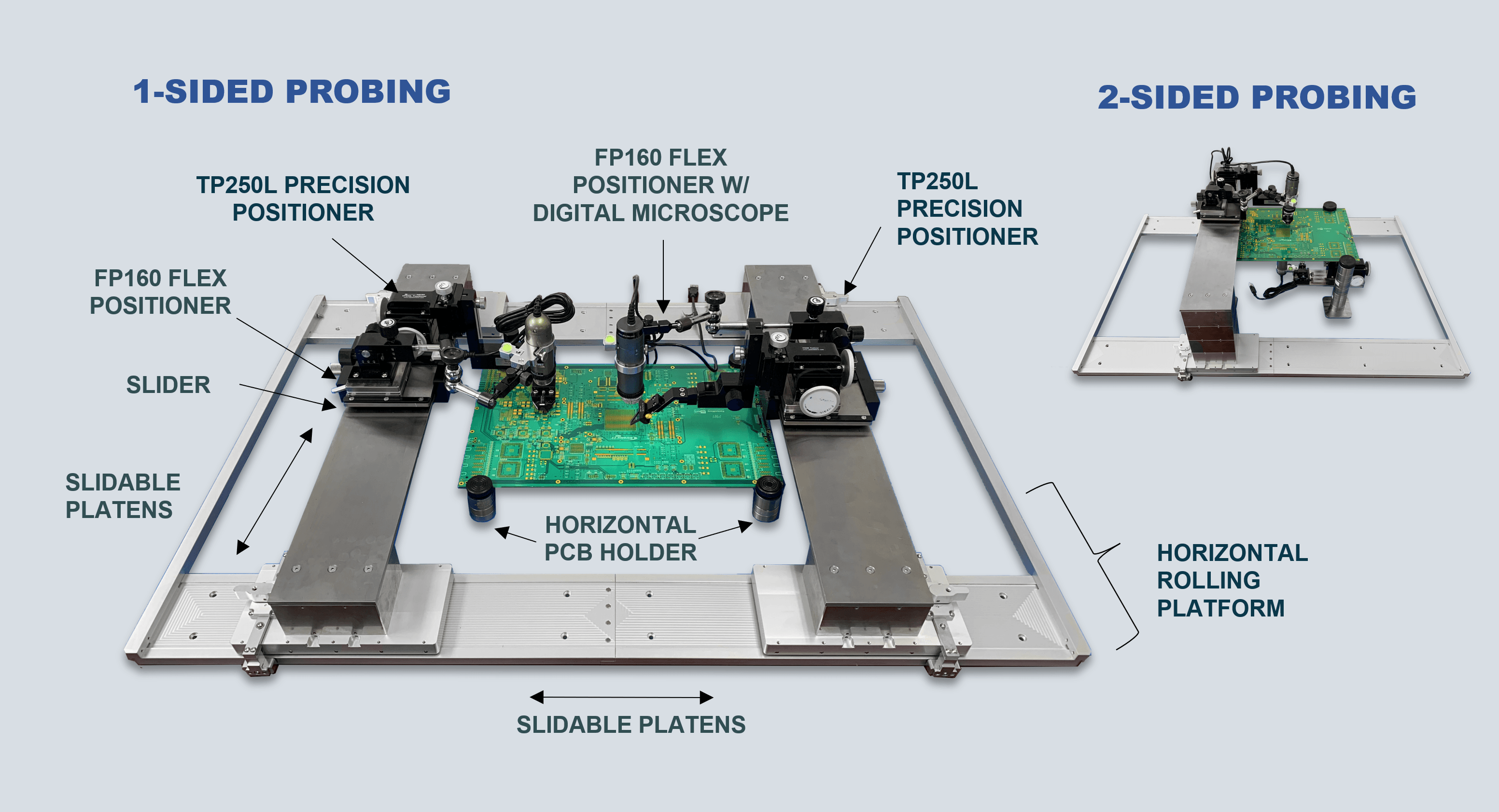
HORIZONTAL PROBE FIXTURE
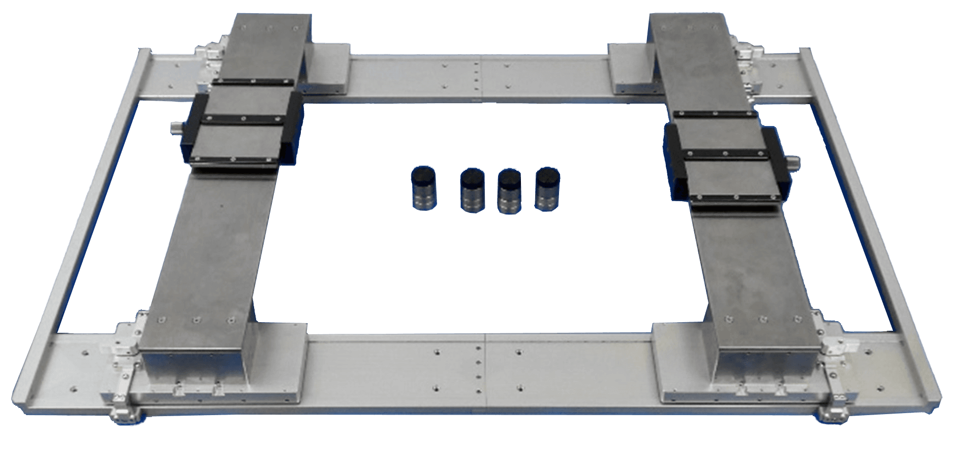
HORIZONTAL PROBE FIXTURE
US Patent 11,125,807
| Specifications | |
|---|---|
| Dimensions HxWxD | 948 x 635 x 330 mm (37.5 x 25 x 4 in) |
| Weight | 22.6 kg (49.6 lb.) |
| Board Size | Height: Max 456 mm (18") Width: unconstrained Thickness: Max 15 mm |
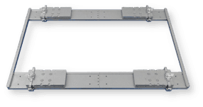
HPF-AR37W25RP4

PB100-24
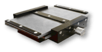
HPF-SL01
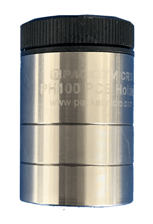
PH100
| PART NUMBERS | QTY | |
|---|---|---|
| Part Group 1 | HPF-AR37 (37" rail) | 2 |
| HPF-RP01(rolling platform) | 4 | |
| HPF-ASB25 (25" spacing bar) | 2 | |
| Part Group 2 | PSP24 (24" Platen) | 2 |
| BL02A (2" blocks) | 4 | |
| BL01A (1" block) | 4 | |
| Slider (HPF-SL01) | Slider for holding TP250 and FP160MS | 2 |
| PCB Holder (PH100) | Horizontal PCB Holder 30 X 40 mm (1.2x1.6") | 4 |
KEY COMPONENTS
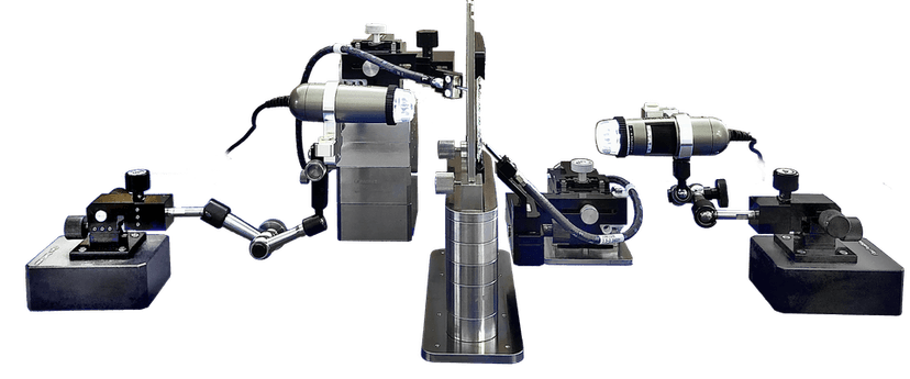
TP250 PRECISION POSITIONER
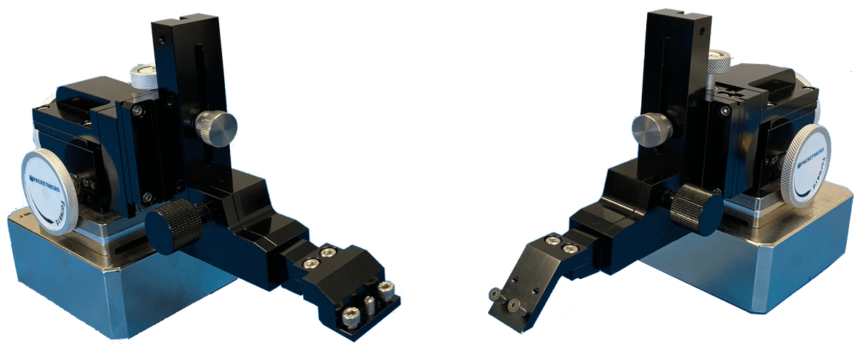
(Left-handed and right-handed shown above) Positioner with various arms and adapters for holding microprobes and PacketMicro probes

FP160MS-MA02
Its built-in 360O adjustable bubble leveler enables the microscope to be correctly oriented at a 900 angle to the PCB. No need to constantly adjust lateral position of the test probe while lowering it to touch down on the test pads.
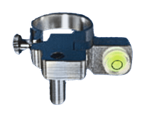
Pull to adjust orientation
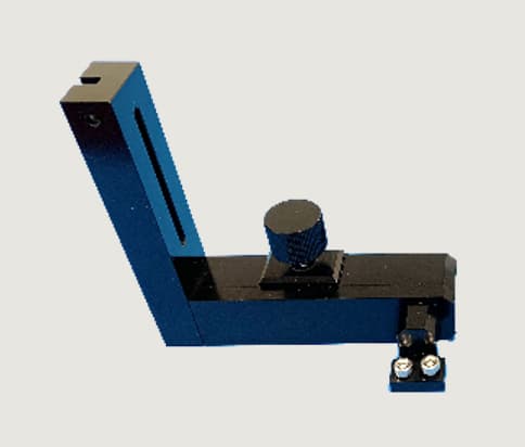
TP250-ARM-AL
Left-handed TP250 arm with PacketMicro 90° probe adapter head
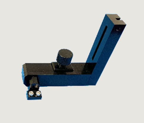
TP250-ARM-AR
Right-handed TP250 arm with PacketMicro 90° probe adapter head
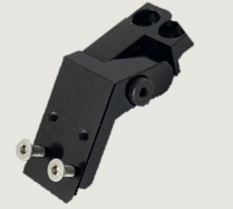
TP250-AVA60
Variable-angle adapter (45°, 60°, 75°)
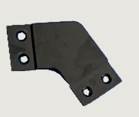
TP250-ABR45
45-degree bracket
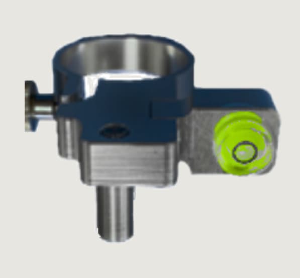
MA02
Microscope Adapter with adjustable level indicator is for holding digital microscope
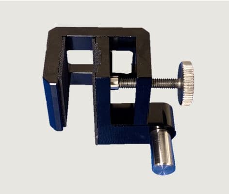
UA16-FP150
Universal adapter can hold large oscilloscope and RF probes.
PROBE STATION CONFIGURATIONS
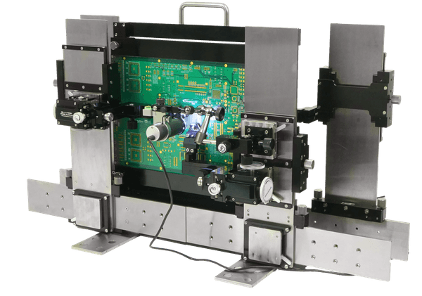
2-SIDED PROBING
HPS24RP can easily be reconfigured for 2-sided probing of large PCBs with additional components.

ADDITIONAL COMPONENTS

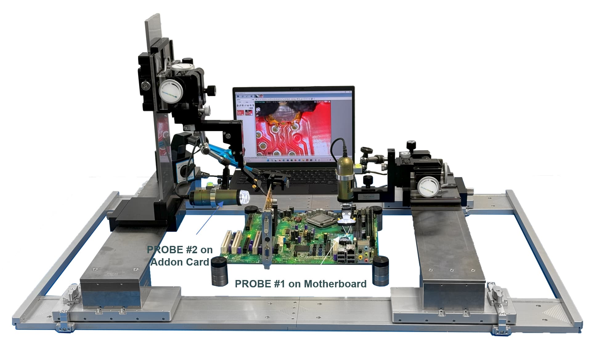
HYBRID PROBING
HPF24RP can also be configured for probing signals between an addon card and a motherboard.
