Challenge
With constant increase in PCB data rate, transmission-line loss becomes important in determining a good or bad PCB. Traditional TDR measurements cannot provide sufficient information of the transmission-line loss. Engineers should consider using a VNA and a de-embedding technique for PCB characterization.
PCB Probing Tips
- Use a test probe assembly with mechanical guide pins. This approach offers fast test time and excellent measurement accuracy.
- Choose a VNA with integrated de-embedding tool to acquire and display real-time transmission-line SnP data.
Helpful Links
Good Practices
- Use test probes instead of RF connectors to reduce PCB test time.
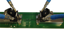
- Design a good probe launch to match the test probes. For example, a probe launch pattern recommended by Intel can accommodate different test probes.
- Use a VNA and 2x Thru de-embedding technique to extract accurate transmission-line s-parameter measurements. Intel Delta-L+ method can be applied for PCB manufacturing qualification at different stages
PCB Characterization Setup

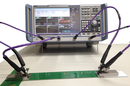
An R&S ZNB20 VNA and two handheld D-Probes are used to test a 20 GHz PCB.

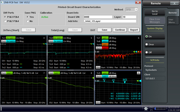
An integrated R&S ZNB20 VNA de-embedding application offers fast real-time measurements and extraction of transmission-line loss.


